����һ���£�AES�㷨��S-box���л�ϵ�Ԫ���Ż���FPGA����ʵ��
����һ���£�Virtex-6 FPGA ML605����������������
ArcticLink�ɱ�����ӽ������ƽ̨����0.18um�������CMOS��������,�ں˵�ѹΪ1.8V,I/O��ѹ���趨Ϊ1.8V,2.5V��3.3V. ArcticLink������ԪΪ640��,�����˸���USB 2.0 OTG������, SD/SDIO/MMC/CE-ATA��������, ASSP/FPGA�ӿ�,�Լ����Ŀɱ�̼ܹ�,�ɱ��I/O,�dz�����ģʽ�Ͱ�ȫ����.���Ľ�����ArcticLink��Ҫ����, �������ƽ̨����ͼ, ���ӽ����������ͼ,�Լ�����USBOTG���ӿ�ͼ����������װ�������ᣬ�����ֻ���PND/PMP��ePOS��Ӧ�ÿ�ͼ��
The QuickLogic ArcticLink Solution Platform is fabricated on a 0.18 ��m, six layer metal CMOS process. The core voltage is 1.8 V. The I/O voltage input tolerance and output drive can be set as 1.8 V, 2.5 V, and 3.3 V.
ArcticLink ��������:
Hi-Speed USB 2.0 OTG Controller
• Single port OTG with embedded high-speed PHY
• Optional 12-signal ULPI interface
• Full-speed CEA-936-A mini-USB analog carkit interface
• Dedicated DMA controller
• High-speed up to 480 Mbits/sec.
SD/SDIO/MMC/CE-ATA Host Controller
• SD/SDIO 1-bit or 4-bit up to 52 MHz with Secure Digital High Capacity (SDHC) support
• CE-ATA 1-bit, 4-bit or 8-bit up to 52 MHz
• MMC 1-bit, 4-bit or 8-bit up to 52 MHz
• High-speed and flexible to support multiple storage options and SDIO peripherals
ASSP/FPGA Interface
• 8 Kbytes scratchpad memory
• Flexible Host interface for USB and SD/SDIO/MMC/CE-ATA ports
• DMA and power management functions
• Direct memory aperture for peripheral subsystems
Flexible Programmable Fabric
• 0.18 ��m, six layer metal CMOS process
• 1.8 V core voltage, 1.8/2.5/3.3 V drive capable I/Os
• 36 Kbits of SRAM �C seven dual-port 4-Kbit high performance SRAM blocks
• Embedded synchronous/asynchronous FIFO controllers
• One user configurable clock manager (CCM) (110-ball WLCSP and 196-ball TFBGA packages only)
• Up to 120 programmable I/Os available
• 100,000 system gates
• Nonvolatile, instant-on
• IEEE 1149.1 boundary scan testing compliant
Programmable I/O
• Bank programmable drive strength
• Bank programmable slew rate control
• Independent I/O banks capable of supporting multiple I/O standards in one device
• Native support for DDRIOs (196-ball package only)
• Bank programmable I/O standards: LVTTL, LVCMOS, and LVCMOS18
• Can be used for level shifter and I/O voltage translator
Very Low Power (VLP) Mode
• The QuickLogic ArcticLink Solution Platform has a special VLP pin which can enable a low power sleep mode that significantly reduces the overall power consumption of the device by placing the device in standby.
• Enter/exit VLP mode from/to normal operation in less than 250 ��s (typical)
Security Links
There are several security links to disable JTAG access to the device. Programming these optional links completely disables access to the device from the outside world and provides an extra level of design security not possible in SRAM-based FPGAs.
JTAG
QuickLogic ArcticLink Solution Platform supports IEEE 1149.1 boundary scan or post-manufacturing testability. External access to this feature can be completely disabled.
ArcticLink QL1A100��Ҫ�����б�: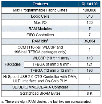

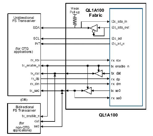
ͼ1.ArcticLink �������ƽ̨����ͼ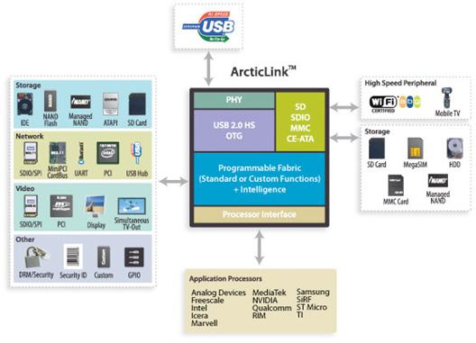
ͼ2.ArcticLink ���ӽ����������ͼ