Virtex®-6 FPGA ML605评估套件The Virtex®-6 FPGA ML605 Evaluation Kit provides a development environment for system designs that demand high-performance, serial connectivity and advanced memory interfacing. The ML605 is supported by pre-verified reference designs and industry-standard FPGA Mezzanine Connectors (FMC) which allow scaling and customization with daughter cards. Integrated tools help streamline the creation of elegant solutions to complex design requirements.
The ML605 board enables hardware and software developers to create or evaluate designs targeting the Virtex®-6 XC6VLX240T-1FFG1156 FPGA.
The ML605 provides board features common to many embedded processing systems. Some commonly used features include: a DDR3 SODIMM memory, an 8-lane PCI Express® interface, a tri-mode Ethernet PHY, general purpose I/O, and a UART. Additional user desired features can be added through mezzanine cards
attached to the onboard high-speed VITA-57 FPGA Mezzanine Connector (FMC) high pin count (HPC) expansion connector, or the onboard VITA-57 FMC low pin count (LPC) connector.
This information includes:• Current version of this user guide in PDF format
• Example design files for demonstration of Virtex-6 FPGA features and technology
• Demonstration hardware and software configuration files for the System ACE™ CF controller, Platform Flash configuration storage device, and linear flash chip
• Reference design files
• Schematics in PDF and DxDesigner formats
• Bill of materials (BOM)
• Printed-circuit board (PCB) layout in Allegro PCB format
• Gerber files for the PCB (Many free or shareware Gerber file viewers are available on the internet for viewing and printing these files.)
• Additional documentation, errata, frequently asked questions, and the latest news
Virtex®-6 FPGA ML605评估套件主要特性:The ML605 provides the following features:
• 1. Virtex-6 XC6VLX240T-1FFG1156 FPGA
• 2. 512 MB DDR3 Memory SODIMM
• 3. 128 Mb Platform Flash XL
• 4. 32 MB Linear BPI Flash
• 5. System ACE CF and CompactFlash Connector
• 6. USB JTAG
• 7. Clock Generation
♦ Fixed 200 MHz oscillator (differential)
♦ Socketed 2.5V oscillator (single-ended)
♦ SMA connectors (differential)
♦ SMA connectors for MGT clocking
• 8. Multi-Gigabit Transceivers (GTX MGTs)
♦ FMC - HPC connector
♦ FMC - LPC connector
♦ SMA
♦ PCIe
♦ SFP Module connector
♦ Ethernet PHY SGMII interface
• 9. PCI Express Endpoint Connectivity
♦ Gen1 8-lane (x8)
♦ Gen2 4-lane (x4)
• 10. SFP Module Connector
• 11. 10/100/1000 Tri-Speed Ethernet PHY
• 12. USB-to-UART Bridge
• 13. USB Controller
• 14. DVI Codec
• 15. IIC Bus
♦ IIC EEPROM - 1 KB
♦ DDR3 SODIMM socket
♦ DVI CODEC
♦ DVI connector
♦ FMC HPC connector
♦ FMC LPC connector
♦ SFP module connector
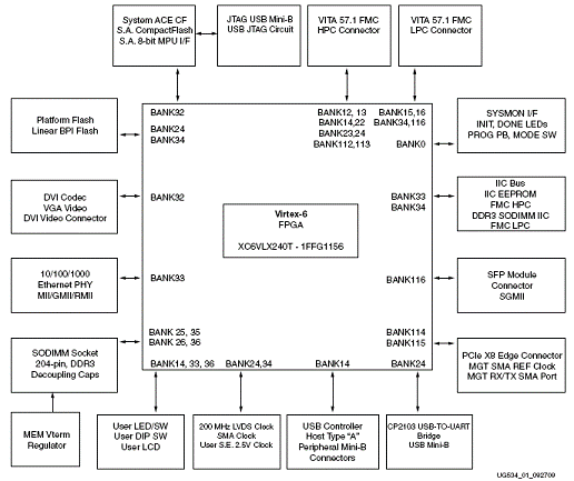
图4.ML605和外设框图
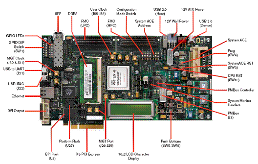
图5.ML605板外形图
上一页 [1] [2] [3]


