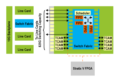
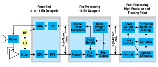
28nm Stratix V FPGA包括增强的核架构,高达28Gbps和低功耗低BER的收发器,以及硬IP区块阵列等. Stratix V FPGA包括四个GT, GX, GS和E系列,内核工作电压0.85V, 533-MHz/1066-Mbps 外接存储器接口, Stratix V GX/GS/E 器件的接口电平为1.2V到3.3V, Stratix V GT 器件的接口电平为1.2V到2.5V, 非常适合用在专注于带宽的应用和协议,40G/100G或更高速率的数据应用以及高性能高精度的DSP应用.本文介绍了Stratix V FPGA系列主要特性,芯片框图以及Stratix V FPGA在100Gb OTN多路收发器, 100GbE线路卡, 纵横制和背板交换, 军用雷, RF卡和通路卡和视频服务器的应用框图以及采用两片Stratix V FPGA的100-GbE线路卡框图.
Altera’s 28-nm Stratix V FPGAs include innovations such as an enhanced core architecture, integrated transceivers up to 28 Gbps, and a unique array of integrated hard intellectual property (IP) blocks. With these innovations, Stratix V FPGAs deliver a new class of application-targeted devices optimized for:
■ Bandwidth-centric applications and protocols
■ Data-intensive applications for 40G/100G and beyond
■ High-performance, high-precision digital signal processing (DSP) applications Stratix V FPGAs are available in four variants (GT, GX, GS, and E), each targeted for a different set of applications. For higher volume production, you can prototype with Stratix V FPGAs and use the low-risk, low-cost path to HardCopy® V ASICs.Stratix V FPGAs deliver the industry’s most flexible transceivers with the highest bandwidth from 600 Mbps to 28 Gbps, low Bit Error Ratio (BER), and low power.
Stratix V transceivers have many enhancements to improve flexibility and robustness.
These enhancements include robust analog receive Clock and Data Recovery (CDR), advanced pre-emphasis and equalization for 12.5 Gbps backplanes. In addition, all transceivers are identical with full featured embedded PCS hard IP to simplify the design, lower the power, and save valuable core resources. Stratix V transceivers are designed to be standard compliant for a wide range of protocols and data rates, and are equipped with a variety of signal conditioning features to support backplane, optical module, and chip-to-chip applications
Stratix V FPGA主要特性:
■ Technology
● 28-nm TSMC process technology
● 0.85-V core voltage
■ Low power serial transceivers
● 28 Gbps transceivers on Stratix V GT devices
● 600 Mbps to 12.5 Gbps backplane capability
● Transmit pre-emphasis and de-emphasis
● Dynamic reconfiguration of individual channels
■ General purpose I/Os
● 1.6-Gbps LVDS
● 533-MHz/1066-Mbps external memory interface
● On-chip termination (OCT)
● 1.2-V to 3.3-V interfacing for Stratix V GX/GS/E devices
● 1.2-V to 2.5-V interfacing for Stratix V GT device
■ Embedded HardCopy Block
● PCI Express Gen1/Gen 2 complete protocol stack, ×1/×4/×8 end point and root port
■ Embedded transceiver hard IP
● Interlaken PCS
● Gigabit Ethernet (GbE) and XAUI PCS
● 10G Ethernet PCS
● Serial Rapid I/O (SRIO) PCS
● Common Public Radio Interface (CPRI) PCS
● Gigabit Passive Optical Networking (GPON) PCS
■ Power Management
● Programmable Power Technology
● Quartus® II integrated PowerPlay Power Analysis
■ High performance core fabric
● Enhanced ALM with 4 registers
● Improved routing architecture reduces congestion and improves compile times
■ Embedded memory blocks
● M20K: 20-Kbit with hard ECC
● MLAB: 640-bit
■ Variable precision DSP blocks
● Up to 500 MHz performance
● Natively support signal processing with precision ranging from 9×9 up to 54×54
● New native 27×27 multiply mode
● 64-bit accumulator and cascade for systolic FIRs
● Embedded internal coefficient memory
● Pre-adder/subtractor improves efficiency
● Increased number of outputs allows more independent multipliers
■ Fractional PLLs
● Fractional mode with third-order delta-sigma modulation
● Integer mode
● Precision clock synthesis, clock delay compensation, and zero delay buffering
■ Clock networks
● 717-MHz fabric clocking
● Global, quadrant, and peripheral clock networks
● Unused clock networks can be powered down to reduce dynamic power
■ Configuration
● Serial and parallel flash interface
● Enhanced AES design security features
● Tamper protection
■ High performance packaging
● Multiple device densities with identical package footprints enables seamless migration between different FPGA densities
● FBGA packaging with on-package decoupling capacitors
● Lead and RoHS-compliant lead-free options
■ HardCopy V migration

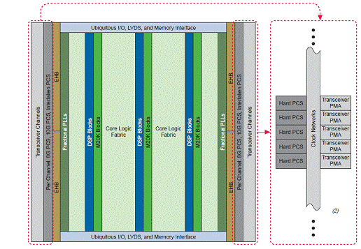
图1。Stratix V GT/GX/GS FPGA芯片图
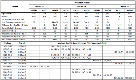
表1。Stratix V GT/GX/GS FPGA型号

Stratix V FPGAs address the design challenges for applications in a variety of industries. Expand the sections below for details about specific applications.
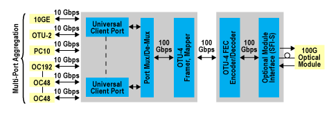
Stratix V GT/GX/GS FPGA应用:1.100-Gb Optical Transport Network (OTN) Multiplexing Transponder

图2.100Gb OTN多路收发器框图
100Gb OTN多路收发器主要特性:
lMulti-standard client interfaces enabled through easy-to-use partial reconfiguration and serial transceivers with continuous data range of 600 Mbps to 12.5 Gbps
lEnhanced clocking flexibility with up to 44 independent transmit clock domains
lIntegrated electronic dispersion compensation (EDC) capability in transceivers to enable direct drive of optical modules (SFP+, SFP, QSFP, CFP)
l28-Gbps transceivers for next-generation optical interfaces
lAdvanced fPLL replacing external voltage-controlled crystal oscillators (VCXOs)
2.100 Gigabit Ethernet (GbE) Line Card

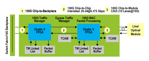
图3.100GbE线路卡框图
100GbE线路卡主要特性:
lHigher system integration through highest density and hard PCS blocks for 40 GbE, 100 GbE, and Interlaken
lHigh-bandwidth data-buffering with up to 1,600-Mbps external memory interfaces
lEfficient implementation of packet processing and traffic management functions
lHigher system performance while staying within your power and cost budget
3.Crossbar and Backplane Switch Fabric

图4.纵横制和背板交换框图
纵横制和背板交换主要特性:
lHighest bandwidth through 66 identical transceivers with continuous data rate from 600 Mbps to 12.5 Gbps
lBuilt-in advanced signal conditioning circuitry for direct drive of 10GBASE-KR backplanes
lFlexible support for various line-card interfaces with partial and dynamic reconfiguration
lOptimized implementation of scheduling functions through high level of integration
4.Military Radar Application

图5.军用雷达应用框图
[1] [2] 下一页
