����BLDC/PMSM��ѹ������Ʒ�������MC9S08AC16ϵ������.����8λMCU������ǿ��HCS08�ں�,���еͳɱ�������,ϵ���и���ģ��,�洢������,�洢�����ͺͷ�װ��ʽ.MC9S08AC16��MC9S08AC8������������Ӻ�ҵ,MC9S08AW16A��MC9S08AW8A������������.���Ľ�����MC9S08AC16ϵ����Ҫ����,����ͼ,�Լ�����BLDC��PMSM��ѹ������Ʒ�����Ҫ����,��ϸ��·ͼ�Լ������嵥(BOM).
3-Phase BLDC/PMSM Low- Voltage Motor Control Drive
The MC9S08AC16 Series devices are members of the low-cost, high-performance HCS08 Family of 8-bit microcontroller units (MCUs). All MCUs in the family use the enhanced HCS08 core and are available with a variety of modules, memory sizes, memory types, and package types.
MC9S08AC16 Series Devices
• Consumer & Industrial
�� MC9S08AC16
MC9S08AC8
• Automotive
�� MC9S08AW16A
�� MC9S08AW8A
8-Bit HCS08 Central Processor Unit (CPU)
• 40-MHz HCS08 CPU (central processor unit)
• 20-MHz internal bus frequency
• HC08 instruction set with added BGND instruction
• Background debugging system
• Breakpoint capability to allow single breakpoint setting during in-circuit debugging (plus two more breakpoints in on-chip debug module)
• Debug module containing two comparators and nine trigger modes. Eight deep FIFO for storing change-of-flow addresses and event-only data. Debug module supports both tag and force breakpoints.
• Support for up to 32 interrupt/reset sources
Memory Options
• Up to 16 KB of on-chip in-circuit programmable FLASH memory with block protection and security options
• Up to 1 KB of on-chip RAM
Clock Source Options
• Clock source options include crystal, resonator, external clock, or internally generated clock with precision NVM trimming
System Protection
• Optional computer operating properly (COP) reset with option to run from independent internal clock source or bus clock
• Low-voltage detection with reset or interrupt
• Illegal opcode detection with reset
• Illegal address detection with reset
Power-Saving Modes
• Wait plus two stops
Peripherals
• ADC �� 8-channel, 10-bit analog-to-digital converter with automatic compare function
• SCI �� Two serial communications interface modules with optional 13-bit break
• SPI �� Serial peripheral interface module
• IIC �� Inter-integrated circuit bus module to operate
at up to 100 kbps with maximum bus loading; capable of higher baud rates with reduced loading
• Timers �� Three 16-bit timer/pulse-width modulator (
TPM) modules �� Two 2-channel and one 4-channel; each has selectable input capture, output compare, and edge-aligned PWM capability on each channel. Each timer module may be configured for buffered,centered PWM (CPWM) on all channels
• KBI �� 7-pin keyboard interrupt module
Input/Output
• Up to 38 general-purpose input/output (I/O) pins
• Software selectable pullups on ports when used as inputs
• Software selectable slew rate control on ports when used as outputs
• Software selectable drive strength on ports when used as outputs
• Master reset pin and power-on reset (POR)
• Internal pullup on RESET, IRQ, and BKGD/MS pins to reduce customer system cost
Package Options
• 48-pin quad flat no-lead package (QFN)
• 44-pin low-profile quad flat package (LQFP)
• 42-pin shrink dual-in-line package (SDIP)
• 32-pin low-profile quad flat package (LQFP)

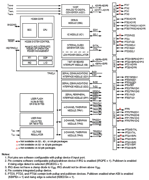
ͼ1.MC9S08AC16ϵ�з���ͼ

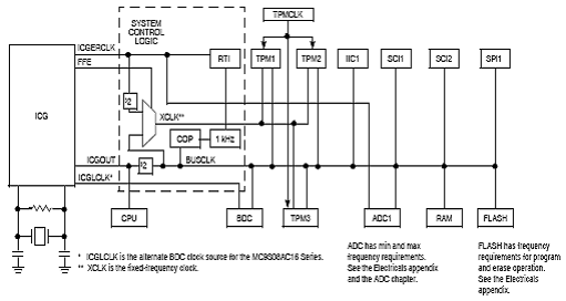
ͼ2.MC9S08AC16ϵͳʱ�ӷֲ�����ͼ
����BLDC/PMSM��ѹ���������������Freescale��s 3-Phase BLDC/PMSM Low-Voltage Motor Control Drive is a 3-phase power stage that will operate with DC input voltages in the range 12�C24 V, 4 A. Together with the daughter boards, it provides a software-development platform that allows algorithms to be written and tested without designing and building any hardware. It supports a variety of algorithms for PMSM and brushless DC (BLDC) motors.
The 3-Phase BLDC/PMSM Low-Voltage Motor Control Drive contains reverse-polarity protection circuitry, MOSFET-gate-drive circuits, analog-signal conditioning, low-voltage power supplies and bridge MOSFETs. The power devices do not need to be mounted on a heatsink.
There are controller daughter boards available with these controllers:
•MC56F8013/23 �� LQFP32
•MC9S08AC16 �� LQFP44
•MCF51AC256 �� LQFP80
•MC9S08MP16 �� LQFP48
•MC56F8006 �� LQFP32
����Ҫ����:•Power supply voltage input 12�C24 V DC, extended up to 50 V (see chapter 2.2 Electrical Characteristics for details)
•Output current 4 A
•Power supply reverse polarity protection circuitry
•3-phase bridge inverter (6 MOSFET��s)
•3-phase MOSFET gate driver with overcurrent and undervoltage protection
•3-phase and DC-bus-current-sensing shunts
•DC-bus voltage sensing
•3-phase back-EMF voltage-sensing circuitry
•Low-voltage on-board power supplies
•Encoder/hall sensor sensing circuitry
•Motor power and signal connectors
•2 connectors for daughter board connection
•CAN physical layer
•USB interface
•User LED, power-on LED, 6 PWM LED diodes, and SCI activity LED diodes
•Up, down, toggle switches
•Reset push-button

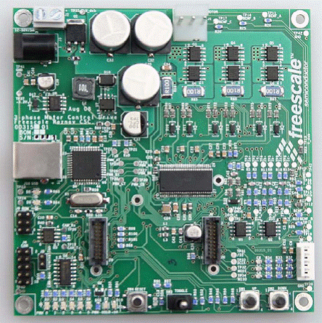
ͼ3.����BLDC/PMSM��ѹ�����������������ͼ

[1] [2] [3] ��һҳ
